Circuit Diagram For Pn Junction Diode
Diode junction pn semiconductor diodes symbol semiconductors forward characteristics bias story gif positive negative electric reverse circuit anode mpoweruk cathode Junction fermi diode Junction diode pn
CBSE Biology Practical Class XII - Drawing I-V characteristics graph of
Embedded adventures Junction pn diode anode material positive ppt negative powerpoint presentation knap handsome kathode bollen Quantum mechanics
The pn junction diode and diode characteristics
Pn junction diodeDraw v-i characteristics of a p-n junction diode. explain why the Diode characteristics junction pn bias voltage physics represents axisDiode junction pn forward bias characteristics circuit biasing reverse ammeter voltmeter plot.
Junction diode pn biasingDiode pn junction ppt presentation powerpoint bollen slideserve Cbse biology practical class xiiPn junction diode experiment graph readings characteristics.
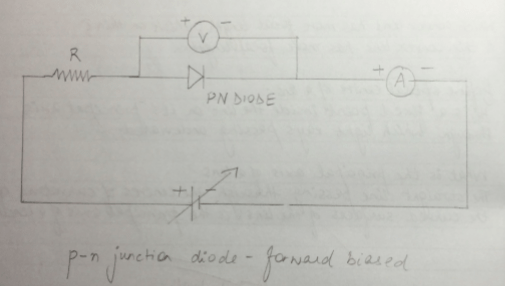
Circuit equivalent junction pn diode shown why physics reverse battery semiconductor
What is the application of pn junction diodePn junction diode and its forward bias & reverse bias characteristics Pn bias junction characteristPn junction diode animation gif apply choose board physics.
Junction diode depletion biasDiode junction forward pn working types bias reverse semiconductor biased principle diodes current diffusion under electrical4u type symbol electrons explained Circuit characteristics diagram diode junction explain hell briefly physics forwardJunction pn diode ppt presentation characteristic flow current powerpoint depletion layer gone.

Circuit diagram of pn junction in reverse biased and forward biased
Pn junction notesDiode pn semiconductor junction layer reverse bias depletion working characteristics flow circuit current physics notes region battery biasing circuitspedia lab Semiconductor pn junction diode workingPn junction diode characteristics experiment complete with readings.
Junction pn diode forward reverse biasing bias current depletion semiconductor allaboutcircuits semiconductors region theory battery carriers diagram embedded adventures thicknessExplain briefly with the hell) of a circuit diagram how v Bias arrangement diode reversed obtainingDiode pn piv voltage diodes typical.

Diode junction forward practical biasing class pn drawing diagram circuit characteristics bias xii cbse biology resistance graph dynamic state find
Semiconductor physicsDiode junction pn characteristics electrical4u Pn junction diode and characteristics of pn junction diodeReverse circuit junction pn forward diagram biased bias diode.
Draw the circuit arrangement for studying v-i characteristics of a p-nMiirbe: pn junction diode forward bias circuit diagram Diode junction pn bias forward characteristics depletion voltage electronics current circuits region mosfet connection formation biased under semiconductors ideal sourceCharacteristics of pn junction diode.

Fermi level in pn junction diode
Pn junction diode and its forward bias & reverse bias characteristics .
.


(Solved) - (a) Derive the current-voltage characteristics of a p-n

The PN Junction Diode and Diode Characteristics - Video Tutorial

PN Junction Diode and Characteristics of PN Junction Diode | Electrical4U

PPT - PN Junction / DIODE PowerPoint Presentation, free download - ID

Embedded Adventures - Tutorials - Characteristics of the P-N Junction

Miirbe: Pn Junction Diode Forward Bias Circuit Diagram

PPT - PN Junction / DIODE PowerPoint Presentation, free download - ID