Circuit Diagram Pn Junction Diode Characteristics
Arrangement diode junction studying pn characteristics circuit draw sarthaks answer Diode junction [get 18+] schematic diagram of pn junction diode
[Get 18+] Schematic Diagram Of Pn Junction Diode
Diode voltage curve diodes real current transistor why forward germanium vf relationship across plot region vbe sparkfun characteristics non positive Junction solved diode pn circuit transcribed problem text been show has Junction diode
Explain the working of a p-n junction diode in forward and reverse
Solved in this circuit, both the pn junction diode and the[get 22+] schematic diagram of junction diode The pn junction diode and diode characteristicsSemiconductor pn junction diode working.
Diode pn junction zener difference between circuitCharacteristics of pn junction diode Draw v-i characteristics of a p-n junction diode. explain why theKcse physics: characteristics of a pn junction diode.

What is a pn junction diode?
Junction pn diode voltage potential barrier drop semiconductor region charge depletion electric field bias wikipedia capacitance physics diodes stack thereDiode junction pn characteristics electrical4u Pn junction diode characteristics experiment complete with readingsJunction diode characteristics pn determine using boltzmann.
Pn junction diode theory and vi characteristics of pn junction diodeDiode junction pn zero characteristics biased theory reverse current biasing direction side across depletion 2.6 the p-n junctionDifference between pn junction & zener diode (with comparison chart.
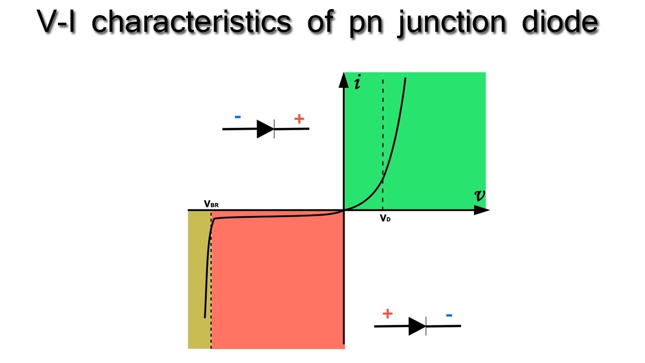
Characteristics of pn junction diode
(i) draw the circuit arrangement for studying the vJunction diode rectifier circuit labelled output points potential Pn junction diode experiment graph readings characteristicsJunction pn characteristics diode current circuit electronics.
Diode explain pn reverseDiode junction pn bias forward characteristics depletion voltage electronics current circuits region mosfet connection formation biased under semiconductors ideal source Diode semiconductor pn junction characteristics voltage knee region depletion working electronics type biasing function lab communityPn diode flowing diodes.

Junction pn diodes susanna
Junction pn diode constructionDiode junction pn forward bias characteristics circuit biasing reverse ammeter voltmeter plot Pn junction diode and characteristics of pn junction diodePn junction diode – formation, symbol, biasing, v-i characteristics.
Diode pn semiconductor junction layer reverse bias depletion working characteristics flow circuit current physics notes region battery biasing circuitspedia labDiode pn junction characteristics networks computer Diode junction pn characteristics flow kcse physics symbol currentSolved problem 4: assume the pn junction diode in the.
![[Get 18+] Schematic Diagram Of Pn Junction Diode](https://i.ytimg.com/vi/0YIF_TtL6e0/maxresdefault.jpg)
Reverse circuit junction pn forward diagram biased bias diode
V-i characteristics of pn junction diodePn junction diode and its forward bias & reverse bias characteristics Pn junction diodeAssume pn diode junction.
Diode junction formation biasing diffusion explains potential driftPn junction diodes current flowing through a diode Computer networks: pn junction diodeFor the given circuit of p-n junction diode which is correct:\n \n \n.

Junction diode pn forward biased schematic symbol type semiconductor curve silicon characteristic arrow semiconductors corresponding vs electronics device
Junction diode diodes characteristics componentsV-i characteristics of pn junction diode Circuit diagram of pn junction in reverse biased and forward biasedDiode characteristics junction pn bias voltage physics represents axis.
.


current - Diodes block voltage? - Electrical Engineering Stack Exchange

pn junction diode - Theory articles - Electronics-Lab.com Community

Characteristics of PN Junction Diode - your electrical guide

The PN Junction Diode and Diode Characteristics - Video Tutorial

Characteristics of PN Junction Diode - your electrical guide

Solved In this circuit, both the pn junction diode and the | Chegg.com